• Hey, guest user. Hope you're enjoying NeoGAF! Have you considered registering for an account? Come join us and add your take to the daily discourse.

Next-Gen PS5 & XSX |OT| Console tEch threaD

Status
Not open for further replies.

Racer!

Member
No, dev kits with final chips. OPN is generally found in chips 6-7 months before retail (in GPU/CPU space) but you would certainly want to have final APU 7-8 months before retail in console space because, unlike retail GPUs and CPUs, you have to provide it to actual developers.

Yes, 7-8 months. Not 18. If PS5 is launching around holiday 2020 that is. Way way too early in my opinion.
 

R600

Banned
Yes, 7-8 months. Not 18. If PS5 is launching around holiday 2020 that is. Way way too early in my opinion.
But the sample actually means you should expect final hardware around February 2020.

OPN sample in GPU/CPU space means final hardware will be provided 6-7 months from when sample was finished so this would mean dev kits with final hardware should be expected by February/March (depending if 1st or 3rd party)
 

R600

Banned
AMD Flute specs read like a bad dream to me if it's PS5

  • Increased latency because GDDR memory not DDR, but half the fucking L3 cache. (Then again CPU latency is MUCH less of an issue in console environment then PC one where many applications and processes depend on latency + GDDR6 sucks for latency anway, so perhaps it would be great to have 16GB of DDR4? Yea, no)
  • Top CPU speed 3.2GHz exactly sweet spot for Zen2 as recent power curve figures shown - perf per watt suffers greatly over 3.3GHZ
  • Only 16GB memory on a 256 bit bus (if clamshell) 256bit bus but fastest memory available - Samsung 18Gbps. Means bandwidth would be 528GB/s if figures from benchmark are anything to go by. Comfortably enough for Zen2 + full Navi.
Not really "nope nope nope". Exactly what we expected, especially after what was shown from Scarlett.
 

xool

Member
Not really "nope nope nope". Exactly what we expected, especially after what was shown from Scarlett.

I didn't think we knew anything about Scarlett - expect some die size and memory guess based on half an image from the promo video .. that may or may not be the real thing ? And are the guess for Scarlett better than this anyway [edit] quote : "estimates ranging from 365 to around 380mm2 .. Navi GPU from AMD clocks in at 251mm2 for 40 of its new compute units, while educated guesses on the size of the eight-core Zen 2 CPU cluster come in at 70-80mm2"(DigitalFoundry) - Scarlett should easily fit full Zen + better than 5700X if true

..latency/L3/256bit bus etc .. but the memory is shared between GPU and CPU .. if the figures in the benchs look inferior right now (compared to a standard 8 core zen) .. imagine what it will look like when the GPU part starts competing for memory ..

Also about the CPU speed - I think 3.2GHz was optimum for .. 3,2GHz DDR4 .. for 16Gb/s GDDR6 I'd expected the "knee" at 4GHz, 3.5GHz for 14Gb/s .. but that's the least of the worries here because it's now sharing memory ..
 
Last edited:

R600

Banned
I didn't think we knew anything about Scarlett - expect some die size and memory guess based on half an image from the promo video .. that may or may not be the real thing ? And are the guess for Scarlett better than this anyway

..latency/L3/256bit bus etc .. but the memory is shared between GPU and CPU .. if the figures in the benchs look inferior right now (compared to a standard 8 core zen) .. imagine what it will look like when the GPU part starts competing for memory ..

Also about the CPU speed - I think 3.2GHz was optimum for .. 3,2GHz DDR4 .. for 16Gb/s GDDR6 I'd expected the "knee" at 4GHz, 3.5GHz for 14Gb/s .. but that's the least of the worries here because it's now sharing memory ..
I am 100% sure we are not getting over 3.2GHZ because at 4.0GHZ, Zen2 uses almost double the energy, while performance benefit is only 15% better. Also, 16MB of cache is half the Zen2 die size, so halving cache will save them quite a bit of space.

Scarlett video shows 330-380mm² chip with 10 GDDR6 14Gbps chips on 320bit bus. 320bit bus will take more space on die, while 14Gbps chips will be slower, therefore actual bandwidth should be relatively close (less then 10% difference).
 
Last edited:
I didn't think we knew anything about Scarlett - expect some die size and memory guess based on half an image from the promo video .. that may or may not be the real thing ? And are the guess for Scarlett better than this anyway

..latency/L3/256bit bus etc .. but the memory is shared between GPU and CPU .. if the figures in the benchs look inferior right now (compared to a standard 8 core zen) .. imagine what it will look like when the GPU part starts competing for memory ..

Also about the CPU speed - I think 3.2GHz was optimum for .. 3,2GHz DDR4 .. for 16Gb/s GDDR6 I'd expected the "knee" at 4GHz, 3.5GHz for 14Gb/s .. but that's the least of the worries here because it's now sharing memory ..

We know that Scarlett is targeting at least 12 TF from specs in early leaks and astroturfer comments from way back when.

This puts Scarlett on 7nm EUV because 7nm DUV tops out around 11 TF.

We also know that MS have backed off from performance leader talk, so I think we can assume they have less than 14.2 TF.
 
Last edited:

THE:MILKMAN

Member
We know that Scarlett is targeting at least 12 TF from specs in early leaks and astroturfer comments from way back when.

This puts Scarlett on 7nm EUV because 7nm DUV tops out around 11 TF.

We also know that MS have backed off from performance leader talk, so I think we can assume they have less than 14.2 TF.

Gotta admire the commitment!

tenor.gif
 

CrustyBritches

Gold Member
The DF Gonzalo vid said it was a QS chip back in April, and that SuborZ+ took around 6-7 months from the time it showed QS until it became a retail product. By that measure we should be seeing this sold in Oct/Nov. If this is a newer QS sample, then that could be pushed to a later date.

I do think Gonzalo = OQA = 20k+ Fire Strike = UserBench leak. I'm less confident it's PS5 than before this Userbench score, but it's long said that DDR4 has better memory latency for applications than something like GDDR5/6. This could all even explain "big, loud towers" with "13TF(probably Vega)" cards, imo.
 
Last edited:

THE:MILKMAN

Member
The DF Gonzalo vid said it was a QS chip back in April, and that SuborZ+ took around 6-7 months from the time it showed QS until it became a retail product. By that measure we should be seeing this sold in Oct/Nov. If this is a newer QS sample, then that could be pushed forward.

I do think Gonzalo = OQA = 20k+ Fire Strike = UserBench leak. I'm less confident it's PS5 than before this Userbench score, but it's long said that DDR4 has better memory latency for applications than something like GDDR5/6. This could all even explain "big, loud towers" with "13TF(probably Vega)" cards, imo.

I think it would help to know the tested dates in 3D Mark for the Pro (Gladius/Gladius B2) and the PS4 (Thebe 9920) to compare them with known dates dev kits where out as well as these Gonzalo January/April/July 2019 dates.
 
done a quick userbench on underclocked Ryzen3700X @3.2Ghz:

userbenchv9ju3.png


comparison mem 3000CL16 non overclocked with 3700X memcontroller at 3.2GHZ and default fabric Clock (Flute on top this time):

userbenchmemh8jvz.png
 
Last edited:

LordOfChaos

Member
why in the world console need multithreading? which takes die space and doesn't give performance increase in games, also turbo clocks isn't necessary in consoles, this sounds more like some kind of laptop to me.

Eh, I hope it keeps SMT, just about every game engine out there knows how to deal with its bit of jitter, and other than that it's a 'free' bit of extra aggregate performance.

As far as die space it would be unlikely that they put the effort into removing it anyways, for the minuscule difference it makes (it was 5% of the die on a Pentium 4, with ever larger logic structures and caches I wouldn't be surprised if it's under a percent of a modern high performance processor)


I don't like that base clock for a console though.
 
Last edited:

IceManCat

Member


Does anyone remember when Cerny negated to use edram to increase bandwith because it would make it too hard for developers? I wonder if he will revisit the idea now with next gen memory and hardware, ssd etc... Just a thought,
 

xool

Member
done a quick userbench on underclocked Ryzen3700X @3.2Ghz:

userbenchv9ju3.png


comparison mem 3000CL16 non overclocked with 3700X memcontroller at 3.2GHZ and default fabric Clock (Flute on top this time):

userbenchmemh8jvz.png
Those Int scores are scarily close .. but again .. not float (inferior scores) - making me thing it's not as good as Zen2. .. If these benchmarks use small data sets that fit in the CPU caches then these figures have meaning .. BUT if they don't then the different memory systems mess up any attempt at comparison.

I looked but couldn't find anything techical about these benchmarks .. so dunno - the explanatory text seems to suggest the benches are supposed to indicate real work performance, not best case math unit throughput - so I assume large data sets .. which sadly makes the comparison fairly meaningless :(

I do think Gonzalo = OQA = 20k+ Fire Strike = UserBench leak. I'm less confident it's PS5 than before this Userbench score,
Connections between the firestrike scores and the userbench marks

  • Firestrike id : ZG16702AE8JB2_32/10/18_13F8
    • Inferred base/boost clock (1.6/3.2GHz) cores (8)
    • Last 4 characters are assume to be PC-ID
  • Userbench id : 100-000000004-15_32/12/18_13F9
    • Clocks/cores match
    • PCI-ID next character along
Problems :

I think it would help to know the tested dates in 3D Mark for the Pro (Gladius/Gladius B2) and the PS4 (Thebe 9920) to compare them with known dates dev kits where out as well as these Gonzalo January/April/July 2019 dates.

There's a search function , https://www.3dmark.com/search , but everything I could think of numbers, codename etc returned 0 results .. why - according to this tweet they have been tested


??
 
Last edited:

xool

Member
It’s not. I think people are just speculating on it because there’s nothing else to do here.

Lots of evidence the thing tested on UserBench has GDDR6 - I don't know of any examples of this outside consoles .. so it's something .. but what ?
 

Racer!

Member
But the sample actually means you should expect final hardware around February 2020.

OPN sample in GPU/CPU space means final hardware will be provided 6-7 months from when sample was finished so this would mean dev kits with final hardware should be expected by February/March (depending if 1st or 3rd party)

You would not need HVM qualified silicon in a devkit a year ahead of launch. Manu for retail would start about 6 months prior. They usually cut those things pretty close, for good reason.

Could be that PS5 launch is closer than anticipated, but I highly doubt it. If PS5 launch with these specs on duv in spring, and Scarlett launch around holiday on euv, it could be a stroke of genius from Microsoft though.
 
Last edited:

SonGoku

Member
of course it's not related there's to much discrepancies to suggest that it is and still some people spin other way around.
i've never believed in gonzalo or second sku for xbox it's fan fiction, from rumor leaks.
Been saying this all along, 8-9TF its just not sufficient for nextgen games at 4k
Unless AMD has plans to release a Gaming APU this is almost certainly a chip for a next-gen console.
Its most likely amd gaming apu for OEMs or SuborZ
unny how this leak matches PCB reddit leak where 32GB of RAM at 256bit bus in clamshell where described (for Devkit).
Which part of this leak? im not seeing any mention of 32GB or clamshell
If you meant because it has 16GB that's no evidence, might as well use Zen2 as evidence lol
Because if they went with 9TF that would be top end of what AMD can provide.
Not really, on DUV they can comfortably provide ~11TF and on EUV 12-13TF
BTW now 3 leaks (Gonzalo, PCB and this new one) tie in perfectly, independently.
Not really, you are really stretching it here: Its has 16GB so it must match!
AMD Flute specs read like a bad dream to me if it's PS5

  • Increased latency because GDDR memory not DDR, but half the fucking L3 cache.
  • Top CPU speed 3.2GHz
  • Only 16GB memory on a 256 bit bus (if clamshell)
nope nope nope
Its not consoles...
 
Last edited:

THE:MILKMAN

Member
There's a search function , https://www.3dmark.com/search , but everything I could think of numbers, codename etc returned 0 results .. why - according to this tweek they have been tested

Believe me I searched it! Apparently others have asked APISAK questions or to clarify about Gonzalo but he doesn't answer?

I assume he has some sort of higher access to 3D Mark?

Would be nice if Richard did an even more detailed look into this but I'm sure he's moved on now.


You would not need HVM qualified silicon in a devkit a year ahead of launch. Manu for retail would start about 6 months prior. They usually cut those things pretty close, for good reason.

Could be that PS5 launch is closer than anticipated, but I highly doubt it. If PS5 launch with these specs on duv in spring, and Scarlett launch around holiday on euv, it could be a stroke of genius from Microsoft though.

PS4 Pro for sure and also I think PS4 had final spec silicon in dev kits ~1 year from launch. We know Pro did because of the date MIC tested the dev kit and then we got the NEO documents leak that stated that specific dev kit was final spec.
 
Last edited:

Racer!

Member
PS4 Pro for sure and also I think PS4 had final spec silicon in dev kits ~1 year from launch. We know Pro did because of the date MIC tested the dev kit and then we got the NEO documents leak that stated that specific dev kit was final spec.

Dont doubt Pro did, but PS4? Thats new to me....source?

Also there is a difference between final spec silicon and silicon ready for HVM.
 
Last edited:


Does anyone remember when Cerny negated to use edram to increase bandwith because it would make it too hard for developers? I wonder if he will revisit the idea now with next gen memory and hardware, ssd etc... Just a thought,


i thought about it before but i don't think it's the right thing to do knowing how well PS4 did, why change the formula .

Have SONY instructed (probably someone at Foxconn) to change codes to prevent leaks ?

Maybe it was the only chip available at the time ?

It’s not. I think people are just speculating on it because there’s nothing else to do here.

(y),i think it's a good track (make sense)
 

THE:MILKMAN

Member
Dont doubt Pro did, but PS4? Thats new to me....source?

Why would you not doubt Pro (using brand new GPU tech still unreleased on PC) having a final silicon a year out but do doubt for PS4?

Anyway, the PS4 was said to have final spec APU in a dev kit from ~ January 2013 for third party (possibly earlier still for Sony?) per VGLeaks.

OrbisDevKit.jpg


Posted on GAF in January 2013. https://www.psdevwiki.com/ps4/DVKT-KS000K-xx_series
 
Needs the RTX5800 or 5900 to support the already promised Ray Tracing.

Gonzalo only has the RTX5700 which doesn’t support Ray Tracing.

it's between RX 5700 - RX 5700xt or if they go with next navi

Pc's are leapfrogging anyway (console ports), (guessing) maybe AMD is planning on releasing Rx 5800xt (56CU's) Rx 5800 (52CU's), lite version (rx 5800) for next gen with (RT) ?

* 52CU @ 1800Mhz = 12 Tf
* 56CU @ 1800Mhz = 12.9 Tf

(console clocks)
* 52CU @ 1550Mhz = 10.3 Tf
* 56CU @ 1550Mhz = 11.1 Tf

navi 10Lite was a test chip (available at the time)

best case scenario.
 

Racer!

Member
Why would you not doubt Pro (using brand new GPU tech still unreleased on PC) having a final silicon a year out but do doubt for PS4?

Anyway, the PS4 was said to have final spec APU in a dev kit from ~ January 2013 for third party (possibly earlier still for Sony?) per VGLeaks.

OrbisDevKit.jpg


Posted on GAF in January 2013. https://www.psdevwiki.com/ps4/DVKT-KS000K-xx_series

That could have been regular engineering samples? There is a difference between final spec hvm qualification retail samples (which is what AMD is labeling with OPN) and final spec engineering samples. Engineering samples can still be manufactured in the thousands for use in testing and devkits.

With Pro they had no new baseline to push/basically they same architecture, work probably started right after PS4. No incentive to cut things close. In addition the tech was basically there, it is after all 2xPS4 with a cpu/gpu clock boost from new node, and a couple of Vega features.
 

THE:MILKMAN

Member
That could have been regular engineering samples? There is a difference between final spec hvm qualification retail samples (which is what AMD is labeling with OPN) and final spec engineering samples. Engineering samples can still be manufactured in the thousands for use in testing and devkits.

With Pro they had no new baseline to push/basically they same architecture, work probably started right after PS4. No incentive to cut things close. In addition the tech was basically there, it is after all 2xPS4 with a cpu/gpu clock boost from new node, and a couple of Vega features.

I guess that makes sense. Although I'm still a little unclear what/where the OPN number is. Is it the 100-000000004 number string? Doesn't tell us much if it is!? Or does it?

The whole Gonzalo timeline is interesting, though. January= ES chip, April= QS chip and July= OPN chip. Has a product gone through these steps and virtually launched before being announced!?
 
Last edited:

Racer!

Member
I guess that makes sense. Although I'm still a little unclear what/where the OPN number is. Is it the 100-000000004 number string? Doesn't tell us much if it is!? Or does it?

The whole Gonzalo timeline is interesting, though. January= ES chip, April= QS chip and July= OPN chip. Has a product gone through these steps and virtually launched before being announced!?

Yes its that first number string.

Why Sony or Microsoft would commit to a hvm sample, throwing away the ability to make changes this early is beyond me. Then again, it could be launching earlier than anyone expects. (PS5)
 
Last edited:

THE:MILKMAN

Member
Yes its that first number string.

Why Sony or Microsoft would commit to a hvm sample, throwing away the ability to make changes this early is beyond me. Then again, it could be launching earlier than anyone expects. (PS5)

Thanks.

The earlier info from insiders/those in the know was that PS5 was coming/aiming for late 2019 but then there was new speculation about a "delay" but that never got confirmed by anyone. Maybe it isn't delayed after all....?
 

THE:MILKMAN

Member
Didn't Cerny confirm its not coming this year?
They wouldn't have skipped E3 otherwise

Not specifically quoted, no. Peter Rubin in his article talks about not expecting this year or it won't be landing in stores anytime in 2019 but Mark isn't quoted saying it. In fact all the quotes from Mark would only be a couple of lines!

I mean it almost certainly isn't coming this year but it would still be a megaton if it came Spring next year for example.


I don't trust this WSJ reporter for stuff he did in the past about Sony/PS5.
 

Racer!

Member
Thanks.

The earlier info from insiders/those in the know was that PS5 was coming/aiming for late 2019 but then there was new speculation about a "delay" but that never got confirmed by anyone. Maybe it isn't delayed after all....?
11.4TF is best case scenario for DUV
On EUV 12-13TF its grounded expectation, 14.2TF dream (but still doable)

Didn't Cerny confirm its not coming this year?
They wouldn't have skipped E3 otherwise

Its not coming this year fiscal (March 2020) as confirmed by that investor meeting. But, could be spring. Also, thats only way I see Sony not going euv. I think this chip is something else though.

My bet is both Sony and Microsoft will launch around holiday 2020, both on euv with Rdna/Rdna2/Zen2 features.
 

SonGoku

Member
but it would still be a megaton if it came Spring next year for example.
It would but i don't think they'll sacrifice performance to release a few months earlier
Its not like they are in any hurry, they can play it smart wait for tech to be affordable for mass production and launch late 2020.
 
Thanks.

The earlier info from insiders/those in the know was that PS5 was coming/aiming for late 2019 but then there was new speculation about a "delay" but that never got confirmed by anyone. Maybe it isn't delayed after all....?

I don't believe 2019 was ever in the running as an actual release date.

It's all been part of a superbly played misinformation campaign.

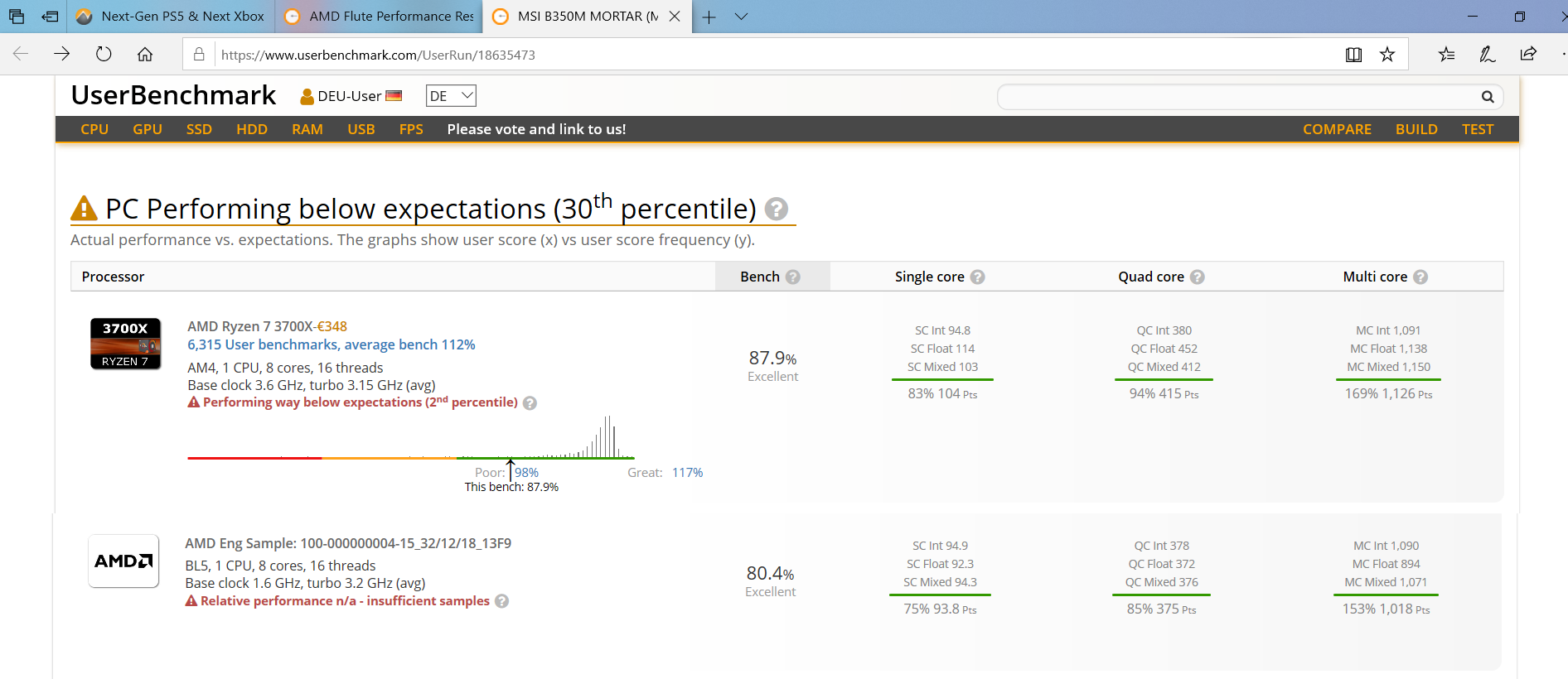
Start whispers of a 2019 release implying a ~8TF 7nm DUV machine.

The competitor hears these whispers and goes for a marginal improvement at the bottom end of the 7nm EUV performance scale. They're confident because 12 TF easily beats 8TF 7nm DUV.

MS fell for it hook, line and sinker. This can be seen from from the early gloating 12TF Anaconda, 8TF PS5 "leaks" and similar astroturfer comments.

Unleash a 14.2 TF beast that utilises the full 7nm EUV die area.

The generation will be won before it even begins.

The final piece of the puzzle is price which will put the last nail in the coffin...
 

R600

Banned
Nice theory, based on thin air, but there where no "8TF" rumors before 2019. It never happened. They have their own targets that where set 3-4 years ago. There is 0% these consoles are using EUV, and even less of a chance they are getting 14.2TF.

14.2TF would be higher performing then ANY GPU currently in existance. And not only that, you would need 512bit bus with 14Gbps chips to feed that beast (or 18Gbps on 384 bit bus). Safe to say, you would be paying through your ass for that one...

Not one of them will deliver double digit TF console.
 

vpance

Member
It would but i don't think they'll sacrifice performance to release a few months earlier
Its not like they are in any hurry, they can play it smart wait for tech to be affordable for mass production and launch late 2020.

Spring 2020 on EUV is my guess. Just as the original rumor had it (Fall 2019 or early 2020).

Launch with Ghosts TLoU2 and 2077. Nextbox would be toast coming out 6 mo later.
 

Racer!

Member
Nice theory, based on thin air, but there where no "8TF" rumors before 2019. It never happened. They have their own targets that where set 3-4 years ago. There is 0% these consoles are using EUV, and even less of a chance they are getting 14.2TF.

14.2TF would be higher performing then ANY GPU currently in existance. And not only that, you would need 512bit bus with 14Gbps chips to feed that beast (or 18Gbps on 384 bit bus). Safe to say, you would be paying through your ass for that one...

Not one of them will deliver double digit TF console.

What do you base this on? In terms of pure economics which is what matters at the end of the day... And how can there be even less than 0% chance of anything?
 
Last edited:

SonGoku

Member
. They have their own targets that where set 3-4 years ago
Correct, nothing prevents those targets from being in the double digits for TF
There is 0% these consoles are using EUV
You don't know that.
14.2TF would be higher performing then ANY GPU currently in existance
Not really, 2080Ti still ahead
By the time consoles launch, 2080Ti will be mid-high range
And not only that, you would need 512bit bus with 14Gbps chips to feed that beast
Not really, a 384 bit bus with 16GBps chips will provide more than enough bandwidth 768GB/s
The 2080TI has 616GB/s for comparison
Not one of them will deliver double digit TF console.
10TF is the absolute minimum either console will target
On DUV ~11TF would be the sweet spot price/perf of a console APU
On EUV 12-13TF
 

R600

Banned
What do you base this on? In terms of pure economics which is what matters at the end of the day...
What matters is when MS and Sony can guarantee that node process will have :

A) acceptable yields
B) acceptable timing for console release

Picking process node for chip design is one of the first thing they do, and i am 100% back in 2016-2017 they targeted 7nm. In addition, consoles used mature process nodes before jumping straight to newest one with questionable yields (and they where, since 3-4 years back they knew very little of EUV yields and if they are even gonna make by then).
 

SonGoku

Member
Spring 2020 on EUV is my guess.
Spring is too early, winter makes more sense for yields and provides enough time to mass produce chips
Not to mention launch games will need every bit of time they can get.

PS4 still has its last power up, with $200 price point and its last 2020 top tier exclusives.
 

R600

Banned
Songoku I am on my phone so its hard to dissect your posts, but we will just have to agree to disagree.

They where coy on TF number and even GPU power in general for a reason. And that is 9TF Navi beats (well matches Vega 7) ANY AMD GPU available today. That means its as good as a get choice for console.

Back in 13' 1.2TF and 1.8TF where equivalent to 5TF and 6.5TF, so we are getting comfortably better this gen.
 

SonGoku

Member
Picking process node for chip design is one of the first thing they do, and i am 100% back in 2016-2017 they targeted 7nm.
7nm EUV fits that timeline
In addition, consoles used mature process nodes before jumping straight to newest one with questionable yields
7nm EUV is not a new process, it uses 4 EUV layers (non critical). Its less complex by nature (cheaper to manufacture) and yields already on par with DUV

There's a reason why all high performing chips skipping DUV
 

SonGoku

Member
Songoku I am on my phone so its hard to dissect your posts, but we will just have to agree to disagree.
Np, take your time
Back in 13' 1.2TF and 1.8TF where equivalent to 5TF and 6.5TF, so we are getting comfortably better this gen.
Im glad you brought this up
Game performance wise going with 8-9TF in 2020 is the equivalent of going with a GTX 280/460 in 2013. Current gen consoles are much better than that
So what is the reason AMD didnt go with EUV with Zen2 and Navi?
Mobile chips this year, big high performance chips next year
btw im not claiming EUV is a done deal, im just pointing out its a realistic possibility that fits the timeline.
 
Last edited:

LordOfChaos

Member
Last edited:
Status
Not open for further replies.
Top Bottom