That's a good point-out, hadn't even thought about the L3$ for CPU in this manner. I'm looking at a Zen 3 diagram and comparing it with the PS5 Zen 2 diagram based on the x-rays; I don't think Sony would be able to have a ringbus around both CCX clusters to simulate a unified L3$, but they could maybe have a buffer between the two 2 MB L3$ clusters on a given CCX...though I'm not sure if that's how it already works with Zen 2 or not (I'm assuming it works that way by default).
So, to explain away performance differences that may be favoring PS5 in most instances atm, I'd chalk it up to either the faster GPU clock speed, lack of issues to sort out due to not having segmented memory spaces, and/or Series X's CPU not being fast enough for keeping the GPU fed with instructions in some sort of way. If there's anything outside of that which could deal with customizations by Sony on the CPU, it would probably be some type of alteration on say maybe the ALUs of the CPU, or some change to the FPU that were able to add in by sacrificing support for lower-latency FADD units. That would be about the extent of it IMO.
Just compare the setup to Navi 21 (also a 40 CU GPU); on Navi 21 you can clearly see IFCC runs along the other parts of the GPU and a central link on both sides connects to both L2$ pools. The L3$ (IC) itself runs parallel around the IFCC; that's the only way you can get the bandwidth, by having the cache (which I'd assume is smaller blocks of cache set parallel around the IFCC, not too dissimilar from the way the L2$ is built from smaller blocks of 256 KB clustered together) each getting a parallel interface along the IFCC.
PS5, from the shots I've seen of the GPU, has no IFCC; even assuming IFCC were in the unified memory controller and whatever sliver of L3$ they could fit between the PHYs connected through it, that would still be a very narrow connection and we already know from the way IFCC and L3$ are arranged on Navi 21 (and surely the other RDNA 2 cards like 6900X) that it's a wide, maybe almost ringbus-style parallel connection for many smaller cache blocks interfaced in parallel. So trying to apply that to PS5, would be small chunks of cache blocks sequentially connected together so only the block immediately interfaced to the controller (with assumed IFCC built in) would actually have a direct link. In other words, data in the cache blocks further down would have to travel sequentially, and there's a latency penalty associated with that.
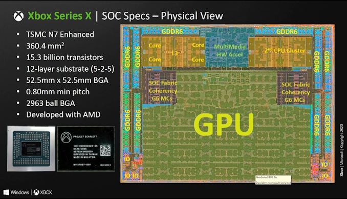
The wide space you are referring to, is probably just general Infinity Fabric to let the CPU and GPU communicate with each other. If you look at the Series X APU schematic, in fact, you will see something similar:
There's similar space between Series X's CPU cores and the GPU, and between the GDDR6 PHYs, yet we already know that system doesn't have IC because, again, there's no presence of an IFCC or pipeline to feed hypothetical IC through to GPU L2$. So we can more or less ascertain that it's exactly similar with Sony's design, otherwise we'd see something more mimicking something similar to 6800 and how its GPU is arranged for IFCC and IC.
K
Kerlurk
I wouldn't necessarily use "blast processing" as an analogy here; MegaDrive actually did have hardware support for direct DMA framebuffer access (something that wasn't standardized with consoles until the Atari Jaguar and then the 5th-gen systems; 3DO might've had it but I'm not sure). The problem was always in figuring the timings, particularly for commercial software, without screwing up game logic.
Hackers and demoscene programmers have managed to figure out the timings though, and there's a lot of demos online showing MegaDrive using "blast processing" in practice; it's actually quite awesome. Wish more commercial games did it though.


 in order soon.