• Hey, guest user. Hope you're enjoying NeoGAF! Have you considered registering for an account? Come join us and add your take to the daily discourse.

Ventura Beat: Nintendo Switch graphics are based on Nvidia's Maxwell Architecture

AgeEighty

Member
I see some reasonable people in here reminding everyone that Pascal is only a bump in efficiency, not in power, but it's like they're shouting into a wind tunnel. It needs to be amplified through the noise:

I have a few immediate thoughts after reading through the article:


  • Firstly, it's worth noting the difference between Maxwell and Pascal is almost entirely down to the manufacturing process. Maxwell was made on 28nm (and in the case of the TX1, 20nm) whereas Pascal is made on 16nm. The actual architectural difference between the two is minimal, and aside from improved color buffer compression, largely irrelevant for a device like the Switch.
  • Despite that, the article never makes any mention of the manufacturing process. I find that extremely strange, as it's obviously the defining difference between the two sets of GPUs.
  • In fact, the article gets the difference between the two completely the wrong way around, saying "Nintendo’s box is relatively small, and so it has to fit into the heat profile of a portable device, rather than a set-top box. That’s another reason that explains the older Maxwell technology, as opposed to the Pascal’s state-of-the-art tech." Pascal is literally a more power efficient version of Maxwell, so the incentive would be the other way around.
  • The author says "we expect the Nintendo Switch to be more than 1 teraflop in performance", which is notably higher than even those of us who were expecting Pascal were considering (I literally posted earlier today with a 500-750 Gflop estimate). If this is a Maxwell chip, then that would mean at least 4 SMs (512 "CUDA cores") at 1GHz, as they're not going to be able to push much past that on 28/20nm. This is a much larger GPU than most people would have been expecting.
I see a few different scenarios here:


  1. The Switch SoC uses Maxwell at 20nm, and simply has a much larger GPU than anticipated to account for the performance.
  2. Nintendo looked at the feature-set planned for Pascal when design started, realised that the new features were largely irrelevant, and decided that they would save time and just use a straight-forward die shrink of Maxwell to 16nm instead. That would technically be a Maxwell GPU, but would be almost completely indistinguishable from Pascal in terms of performance.
  3. The sources are wrong about Maxwell, the 1 Tflop performance, or both.
Basically, if you're to take the article as being accurate, then the only worthwhile takeaway is this quote:


A Maxwell Tflop is identical to a Pascal Tflop, and it's largely irrelevant to us whether they achieved that by using a larger Maxwell GPU on 20nm/28nm at a lower clock or a smaller Pascal GPU on 16nm at a higher clock.
 

imjust1n

Banned
This system is not 9th Generation guys this is still 8th Gen. Why are you expecting 4k gaming on a tablet? I think you need to evaluate your expectations down alot if you are hyping yourself thinking its going to play next gen games at 4k res. Im sure most games will run but it just wont be full 1080p. Also that screen only is a 720p screen so.....its only gonna going to run 720p.
 
Using cheaper, older parts is a very Nintendo thing to do. I don't know why anyone expected differently.

Because Pascal is actually cheaper than Maxwell because it uses a lot less space and material.

Or, in order to try to help clarify things- a newer 16nm process is cheaper than an older 20nm process.
 

Elios83

Member
Maxwell vs Pascal has more to do with power efficiency and perfomance/watt.
It seems weird that a console with handheld ambitions has a chip based on a less power efficient architecture. For the same floating point calculation speed they'd get more heat and less battery life.
If nVidia has fucked Nintendo (after they did the same with Sony and Microsoft for different reasons) giving them a variant of the Tegra used in the Shield with the excuse that Pascal was not ready...LOL.
 

Vena

Member
The author says "we expect the Nintendo Switch to be more than 1 teraflop in performance", which is notably higher than even those of us who were expecting Pascal were considering (I literally posted earlier today with a 500-750 Gflop estimate). If this is a Maxwell chip, then that would mean at least 4 SMs (512 "CUDA cores") at 1GHz, as they're not going to be able to push much past that on 28/20nm. This is a much larger GPU than most people would have been expecting.
...
The sources are wrong about Maxwell, the 1 Tflop performance, or both.

The 1TFLOP number seems to be the most dubious detail here, because it could very easily be a confused FP16 performance benchmark, and the rest of the article gives no confidence that the author has a firm grip of the general technical details to make the distinction.
 

keakster

Member
I have a few immediate thoughts after reading through the article:

...

I see a few different scenarios here:

  1. The Switch SoC uses Maxwell at 20nm, and simply has a much larger GPU than anticipated to account for the performance.
  2. Nintendo looked at the feature-set planned for Pascal when design started, realised that the new features were largely irrelevant, and decided that they would save time and just use a straight-forward die shrink of Maxwell to 16nm instead. That would technically be a Maxwell GPU, but would be almost completely indistinguishable from Pascal in terms of performance.
  3. The sources are wrong about Maxwell, the 1 Tflop performance, or both.

A Maxwell Tflop is identical to a Pascal Tflop, and it's largely irrelevant to us whether they achieved that by using a larger Maxwell GPU on 20nm/28nm at a lower clock or a smaller Pascal GPU on 16nm at a higher clock.

Thank you for this
 

J@hranimo

Banned
I have a few immediate thoughts after reading through the article:


  • Firstly, it's worth noting the difference between Maxwell and Pascal is almost entirely down to the manufacturing process. Maxwell was made on 28nm (and in the case of the TX1, 20nm) whereas Pascal is made on 16nm. The actual architectural difference between the two is minimal, and aside from improved color buffer compression, largely irrelevant for a device like the Switch.
  • Despite that, the article never makes any mention of the manufacturing process. I find that extremely strange, as it's obviously the defining difference between the two sets of GPUs.
  • In fact, the article gets the difference between the two completely the wrong way around, saying "Nintendo’s box is relatively small, and so it has to fit into the heat profile of a portable device, rather than a set-top box. That’s another reason that explains the older Maxwell technology, as opposed to the Pascal’s state-of-the-art tech." Pascal is literally a more power efficient version of Maxwell, so the incentive would be the other way around.
  • The author says "we expect the Nintendo Switch to be more than 1 teraflop in performance", which is notably higher than even those of us who were expecting Pascal were considering (I literally posted earlier today with a 500-750 Gflop estimate). If this is a Maxwell chip, then that would mean at least 4 SMs (512 "CUDA cores") at 1GHz, as they're not going to be able to push much past that on 28/20nm. This is a much larger GPU than most people would have been expecting.
I see a few different scenarios here:


  1. The Switch SoC uses Maxwell at 20nm, and simply has a much larger GPU than anticipated to account for the performance.
  2. Nintendo looked at the feature-set planned for Pascal when design started, realised that the new features were largely irrelevant, and decided that they would save time and just use a straight-forward die shrink of Maxwell to 16nm instead. That would technically be a Maxwell GPU, but would be almost completely indistinguishable from Pascal in terms of performance.
  3. The sources are wrong about Maxwell, the 1 Tflop performance, or both.
Basically, if you're to take the article as being accurate, then the only worthwhile takeaway is this quote:


A Maxwell Tflop is identical to a Pascal Tflop, and it's largely irrelevant to us whether they achieved that by using a larger Maxwell GPU on 20nm/28nm at a lower clock or a smaller Pascal GPU on 16nm at a higher clock.

This needs to be in the OP stat! Thank you good person, this spells it out nicely.
 

Polygonal_Sprite

Gold Member
You know, another funny thing is that they're expecting something almost on-par with Xbone yet at the same time say that it's too weak for Xbone games.

What I can say for certain is that they only heard about the architecture and nothing else, and everything else is just uninformed guessing.

Also, I want to remind you that 20nm and 16nmFF are identical in terms of transistor density.

Have you read the whole article ? The whole thing seems like speculation filled with misinformation and spelling mistakes like "Xbox Skorpio" lol.
 
I see some reasonable people in here reminding everyone that Pascal is only a bump in efficiency, not in power, but it's like they're shouting into a wind tunnel. It needs to be amplified through the noise:
Even the Judas traitor Nate Drake said that ages ago when he revealed from his corrupt abominable sources that the Switch would be using Pascal and everyone naively popped grafx boners.
 

Instro

Member
I have a few immediate thoughts after reading through the article:


  • Firstly, it's worth noting the difference between Maxwell and Pascal is almost entirely down to the manufacturing process. Maxwell was made on 28nm (and in the case of the TX1, 20nm) whereas Pascal is made on 16nm. The actual architectural difference between the two is minimal, and aside from improved color buffer compression, largely irrelevant for a device like the Switch.
  • Despite that, the article never makes any mention of the manufacturing process. I find that extremely strange, as it's obviously the defining difference between the two sets of GPUs.
  • In fact, the article gets the difference between the two completely the wrong way around, saying "Nintendo’s box is relatively small, and so it has to fit into the heat profile of a portable device, rather than a set-top box. That’s another reason that explains the older Maxwell technology, as opposed to the Pascal’s state-of-the-art tech." Pascal is literally a more power efficient version of Maxwell, so the incentive would be the other way around.
  • The author says "we expect the Nintendo Switch to be more than 1 teraflop in performance", which is notably higher than even those of us who were expecting Pascal were considering (I literally posted earlier today with a 500-750 Gflop estimate). If this is a Maxwell chip, then that would mean at least 4 SMs (512 "CUDA cores") at 1GHz, as they're not going to be able to push much past that on 28/20nm. This is a much larger GPU than most people would have been expecting.
I see a few different scenarios here:


  1. The Switch SoC uses Maxwell at 20nm, and simply has a much larger GPU than anticipated to account for the performance.
  2. Nintendo looked at the feature-set planned for Pascal when design started, realised that the new features were largely irrelevant, and decided that they would save time and just use a straight-forward die shrink of Maxwell to 16nm instead. That would technically be a Maxwell GPU, but would be almost completely indistinguishable from Pascal in terms of performance.
  3. The sources are wrong about Maxwell, the 1 Tflop performance, or both.
Basically, if you're to take the article as being accurate, then the only worthwhile takeaway is this quote:


A Maxwell Tflop is identical to a Pascal Tflop, and it's largely irrelevant to us whether they achieved that by using a larger Maxwell GPU on 20nm/28nm at a lower clock or a smaller Pascal GPU on 16nm at a higher clock.

I would assume they just mistook FP16 and FP32 performance.

I see some reasonable people in here reminding everyone that Pascal is only a bump in efficiency, not in power, but it's like they're shouting into a wind tunnel. It needs to be amplified through the noise:

Well yes, but a bump in efficiency allows the device to be driven at a higher speed.
 

Schnozberry

Member
NTD operates in conjunction with Nintendo PTD. So while Sudharsan and the Redmond team research and develop a lot of technology, the Japan arm (Platform Technology & Development Division) is still the lead developer.

Ko Shiota is the head of PTD, and was the right hand man of Takeda. But even before all that, the big decisions of the hardware were probably still made at the end of the Iwata/Takeda/Miyamoto reign back in early 2015?

Major design decisions are always run up the flag pole in any organization. The timing may be coincidental, but given his previous experience at Nvidia, it seems pretty fortuitous for Sudha to get a promotion to head NTD in early 2016 after Switch design would have likely been in its final stages. From presentation all the way down to the look and feel of the hardware, the Switch seems like a pivot towards more western design influence.

The purported use of Maxwell may have just came down to timing. If true, it becomes easy to believe this was initially going to be a Holiday 2016 device.
 

ggx2ac

Member
Also, I want to remind you that 20nm and 16nmFF are identical in terms of transistor density.

Is there a difference between transistor count and transistor density?

For example, a TX1 die shrunk from 20nm to 16nm would have the same transistor count but, it's density would increase per m³ which allows for the reduction in power consumption.
Wouldn't it?
 

NateDrake

Member
I appreciate your efforts but your reporting on NVidia Pascal in the final system formed the basis of much of your credibility regarding Switch. It's the factoid that we tend to cite the most when we're asked what you've gotten right. It would be very unfortunate if it turned out to be Maxwell. I personally would feel disappointed and misled.

It will be what it'll be. I'm not going to hide behind "speculation" or "educated guess" because this wasn't any of that. I had well-placed sources that informed me of Pascal during the summer. I know for fact it was considered and investigated for use with Switch.
 
D

Deleted member 465307

Unconfirmed Member
If Switch ends up using a chip that's a customized version of Maxwell, that sounds like an architectural sidestep of Pascal (like if Pascal were developed in another timeline), given what Pascal's relationship to Maxwell is. I guess what it will come down to is the process node. Hopefully Nintendo went with 16nm, but the worst case scenario is probably 20nm anyway.

This article's performance estimations should change the mind of no one who was following the Switch rumors because it's exactly in line with what we've been hearing for months.

Also, good post, Thraktor!
 

HAL-01

Member
Very skeptical of those sources. Not only does this leak contradict all other info out there, it also comes with a little story justifying why nintendo did it, which doesn't really happen with actual hardware leaks.
real fishy.
That said, no one should expect this to be Xbox one level. Expect 60% at most, when docked.
 

MuchoMalo

Banned
Have you read the whole article ? The whole thing seems like speculation filled with misinformation and spelling mistakes like "Xbox Skorpio" lol.

Honestly, I read the first page of this thread, the responses annoyed me, I remembered why I haven't been on Gaf much lately and posted a kneejerk response to the kneejerk responses. I don't really care much since it doesn't really affect my expectations either way.

Is there a difference between transistor count and transistor density?

For example, a TX1 die shrunk from 20nm to 16nm would have the same transistor count but, it's density would increase per m³ which allows for the reduction in power consumption.
Wouldn't it?

It's the move to FinFET that increases efficiency. 16nmFF could easily be called 20nmFF and still be correct.
 

Vena

Member
It will be what it'll be. I'm not going to hide behind "speculation" or "educated guess" because this wasn't any of that. I had well-placed sources that informed me of Pascal during the summer. I know for fact it was considered and investigated for use with Switch.

I mean, isn't even just that much already at odds with this article? Article makes it sound like they completely omitted Pascal consideration for timetables.
 

AgeEighty

Member
Well yes, but a bump in efficiency allows the device to be driven at a higher speed.

Which was never going to happen in a portable device.

If people are going to be upset about Maxwell instead of Pascal (if this report is accurate), it should be for reasons of battery life, not graphics performance.
 
It will be what it'll be. I'm not going to hide behind "speculation" or "educated guess" because this wasn't any of that. I had well-placed sources that informed me of Pascal during the summer. I know for fact it was considered and investigated for use with Switch.

To be fair your sources may have heard 16nm process and conflated that with Pascal like many people in this thread are doing. The latest devkits could easily have Maxwell architecture on a 16nm process, effectively giving it all of the benefits of Pascal, so you'd be -for all intents and purposes- correct.
 
It will be what it'll be. I'm not going to hide behind "speculation" or "educated guess" because this wasn't any of that. I had legit and well-placed sources that informed me of Pascal during the summer. I know for fact it was considered and investigated for use with Switch.
You should have worded your revelation exactly that way then.
I personally don't see it as a big deal but
~crosses NateDrake's sources off the blackboard of saving the Switch~
 

AR15mex

Member
The funny thing is that nvidia mentions on their PR that tegra is based on pascal so does this gets automatically debunked...?

Edit: add quote from nvidia

Nintendo Switch is powered by the performance of the custom Tegra processor. The high-efficiency scalable processor includes an NVIDIA GPU based on the same architecture as the world’s top-performing GeForce gaming graphics cards

So it maybe possible due to the fact that they say top cards but maybe they are including maxwell arquitecture as top end as well?
 
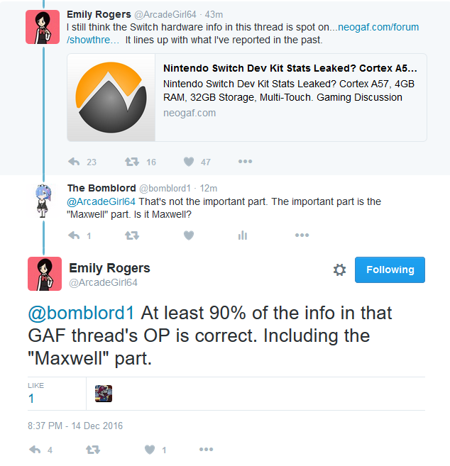
Who does it contradict? Emily agrees with Maxwell

All Emily is saying is that the devkits she heard about in August had a Maxwell chip in them. But even the original Eurogamer leak said that could be a placeholder. As far as I can tell, Emily isn't confirming that final retail units use Maxwell, which is what VentureBeat is doing here. However there are people saying final units will be Pascal, and I believe that is the contraction poster is referring to.
 

LCGeek

formerly sane
The funny thing is that nvidia mentions on their pr that tegra is based on pascal so... does this gets automatically debunked...

Was gonna bring that up, cause nintendo should be pissed if nintendo is being two faced. The rumor really doesn't jive in some areas as thraktor mentioned so hopefully people know to ignore VB on certain shit and move on.

VB is dumb if they think dev kits automatically equal retail units when history on the last 3 nintendo consoles says otherwise.
 

chaosblade

Unconfirmed Member
I didn't even think Maxwell supported FP16 but it looks like it was added to V2 or whatever. Regardless, isn't FP16 mostly useless for games? At least that's what I recall reading.
 

NateDrake

Member
Was gonna bring that up, cause nintendo should be pissed if nintendo is being two faced. The rumor really doesn't jive in some areas as thraktor mentioned so hopefully people know to ignore VB on certain shit and move on.

VB is dumb if they think dev kits automatically equal retail units when history on the last 3 nintendo consoles says otherwise.

I know the final dev kits are using Maxwell. If my Pascal information is inaccurate, I'll certainly own up to it. I shared it at a time I was extremely confident in the information.
 

_woLf

Member
Legitimately huge mistake if true. Need Pascal to stay competitive in a couple years.

Very very disappointing.
 

Terrell

Member
Was gonna bring that up, cause nintendo should be pissed if nintendo is being two faced. The rumor really doesn't jive in some areas as thraktor mentioned so hopefully people know to ignore VB on certain shit and move on.

VB is dumb if they think dev kits automatically equal retail units when history on the last 3 nintendo consoles says otherwise.

Any piece of "confirmed information" they could get their hands on to justify the clickbait headline they've clearly wanted to use for a while now.
 

AgeEighty

Member
Who does it contradict? Emily agrees with Maxwell

She's agreeing with the "It won't be as powerful as a PS4" headline. And she says 90% of the devkit specs on Robert's thread are accurate, but she doesn't say which 10% aren't. EDIT: Corrected below.

I mean, using Pascal wouldn't make Switch as powerful as a PS4 either.
 
Was gonna bring that up, cause nintendo should be pissed if nintendo is being two faced. The rumor really doesn't jive in some areas as thraktor mentioned so hopefully people know to ignore VB on certain shit and move on.

VB is dumb if they think dev kits automatically equal retail units when history on the last 3 nintendo consoles says otherwise.

Apparently this author is fairly trustworthy so I don't know if I would outright dismiss his sources, but his conclusions in the article are almost nonsense, so he clearly doesn't know the implications of Maxwell vs Pascal. Which, if we are ignoring the process node, are essentially nothing at all.

So it wouldn't surprise me to see the final SoC have Maxwell architecture on a 16nm process, which would agree with his sourced info. But it would disagree largely with his conclusions.
 

phanphare

Banned
She's agreeing with the "It won't be as powerful as a PS4" headline. And she says 90% of the devkit specs on Robert's thread are accurate, but she doesn't say which 10% aren't.

she later confirms the maxwell part but the context is that she's referring to the dev kit specs, which has been known
 

bomblord1

Banned
She's agreeing with the "It won't be as powerful as a PS4" headline. And she says 90% of the devkit specs on Robert's thread are accurate, but she doesn't say which 10% aren't.

capturemfk5j.png
 

AgeEighty

Member
she later confirms the maxwell part but the context is that she's referring to the dev kit specs, which has been known

Thanks, I'd missed that. But yes, still meaningless in the context of retail units and in the context of Switch's graphical performance.
 

LordOfChaos

Member
I see some reasonable people in here reminding everyone that Pascal is only a bump in efficiency, not in power, but it's like they're shouting into a wind tunnel. It needs to be amplified through the noise:


If you have (say) 5 watts to work with, a bump in efficiency IS a bump in power.

Boiled down you can say power draw x efficiency = performance, if power draw is set by chassis size and battery capacity, you increase performance with what?

This is true in even higher wattage spaces.

Intel learned this. Nvidia learned this. AMD is getting there.

Pascal is far from a straight die shrink of Maxwell 2 either, that's quite uncharitable to the effort. And I don't see compression being irrelevant to the switch, I see it being pivotal for limited mobile bandwidth.

http://www.anandtech.com/show/10325/the-nvidia-geforce-gtx-1080-and-1070-founders-edition-review/2
 

AgeEighty

Member
If you have (say) 5 watts to work with, a bump in efficiency IS a bump in power.

This is true in even higher wattage spaces.

Intel learned this. Nvidia learned this. AMD is getting there.

It's highly unlikely that they ever would have used that extra power for a graphical boost on a portable machine that already reportedly has poor battery life.
 
If you have (say) 5 watts to work with, a bump in efficiency IS a bump in power.

This is true in even higher wattage spaces.

Intel learned this. Nvidia learned this. AMD is getting there.

But just saying Maxwell without mentioning the fabrication process does not tell us whether or not it will get that bump in efficiency. I think this is the major reason to ignore the article- you can have 16nm Maxwell and it would not technically be Pascal, though fairly similar.

But it makes no difference performance wise. So it tells us nothing new.

It's highly unlikely that they ever would have used that extra power for a graphical boost on a portable machine that already reportedly has poor battery life.

The graphical boost comes into play when docked. Also the current battery life rumor is that they're targeting 5 hours as the minimum.
 

Eliseo

Member
I have a few immediate thoughts after reading through the article:


  • Firstly, it's worth noting the difference between Maxwell and Pascal is almost entirely down to the manufacturing process. Maxwell was made on 28nm (and in the case of the TX1, 20nm) whereas Pascal is made on 16nm. The actual architectural difference between the two is minimal, and aside from improved color buffer compression, largely irrelevant for a device like the Switch.
  • Despite that, the article never makes any mention of the manufacturing process. I find that extremely strange, as it's obviously the defining difference between the two sets of GPUs.
  • In fact, the article gets the difference between the two completely the wrong way around, saying "Nintendo’s box is relatively small, and so it has to fit into the heat profile of a portable device, rather than a set-top box. That’s another reason that explains the older Maxwell technology, as opposed to the Pascal’s state-of-the-art tech." Pascal is literally a more power efficient version of Maxwell, so the incentive would be the other way around.
  • The author says "we expect the Nintendo Switch to be more than 1 teraflop in performance", which is notably higher than even those of us who were expecting Pascal were considering (I literally posted earlier today with a 500-750 Gflop estimate). If this is a Maxwell chip, then that would mean at least 4 SMs (512 "CUDA cores") at 1GHz, as they're not going to be able to push much past that on 28/20nm. This is a much larger GPU than most people would have been expecting.
I see a few different scenarios here:


  1. The Switch SoC uses Maxwell at 20nm, and simply has a much larger GPU than anticipated to account for the performance.
  2. Nintendo looked at the feature-set planned for Pascal when design started, realised that the new features were largely irrelevant, and decided that they would save time and just use a straight-forward die shrink of Maxwell to 16nm instead. That would technically be a Maxwell GPU, but would be almost completely indistinguishable from Pascal in terms of performance.
  3. The sources are wrong about Maxwell, the 1 Tflop performance, or both.
Basically, if you're to take the article as being accurate, then the only worthwhile takeaway is this quote:


A Maxwell Tflop is identical to a Pascal Tflop, and it's largely irrelevant to us whether they achieved that by using a larger Maxwell GPU on 20nm/28nm at a lower clock or a smaller Pascal GPU on 16nm at a higher clock.

More people needs to see this.
 
This isn't too surprising. I think the Zelda demo they showed on Fallon looked rough to say the least. It'll probably run PS360-esque games no problem but I doubt it can match the PS4.
 
I have a few immediate thoughts after reading through the article:


  • Firstly, it's worth noting the difference between Maxwell and Pascal is almost entirely down to the manufacturing process. Maxwell was made on 28nm (and in the case of the TX1, 20nm) whereas Pascal is made on 16nm. The actual architectural difference between the two is minimal, and aside from improved color buffer compression, largely irrelevant for a device like the Switch.
  • Despite that, the article never makes any mention of the manufacturing process. I find that extremely strange, as it's obviously the defining difference between the two sets of GPUs.
  • In fact, the article gets the difference between the two completely the wrong way around, saying "Nintendo’s box is relatively small, and so it has to fit into the heat profile of a portable device, rather than a set-top box. That’s another reason that explains the older Maxwell technology, as opposed to the Pascal’s state-of-the-art tech." Pascal is literally a more power efficient version of Maxwell, so the incentive would be the other way around.
  • The author says "we expect the Nintendo Switch to be more than 1 teraflop in performance", which is notably higher than even those of us who were expecting Pascal were considering (I literally posted earlier today with a 500-750 Gflop estimate). If this is a Maxwell chip, then that would mean at least 4 SMs (512 "CUDA cores") at 1GHz, as they're not going to be able to push much past that on 28/20nm. This is a much larger GPU than most people would have been expecting.
I see a few different scenarios here:


  1. The Switch SoC uses Maxwell at 20nm, and simply has a much larger GPU than anticipated to account for the performance.
  2. Nintendo looked at the feature-set planned for Pascal when design started, realised that the new features were largely irrelevant, and decided that they would save time and just use a straight-forward die shrink of Maxwell to 16nm instead. That would technically be a Maxwell GPU, but would be almost completely indistinguishable from Pascal in terms of performance.
  3. The sources are wrong about Maxwell, the 1 Tflop performance, or both.
Basically, if you're to take the article as being accurate, then the only worthwhile takeaway is this quote:


A Maxwell Tflop is identical to a Pascal Tflop, and it's largely irrelevant to us whether they achieved that by using a larger Maxwell GPU on 20nm/28nm at a lower clock or a smaller Pascal GPU on 16nm at a higher clock.

Also, why does a source that knows something as intricate as the architecture of the GPU not even have any information regarding whether or not the device has a touchscreen? In the article it says that it's up in the air. I find it hard to believe they would have multiple sources know such a narrow scop of informstuon when a touchscreen would be a pretty basic fact for somebody involved with the system.
 
Most people already knew and had accepted it wouldn't be as powerful as PS4. It's been widely reported for months and months. I don't see how this article could surprise most people.

How would Pascal be in the Switch, be able to run cool, and be able to be sold for less than $300?
 

Jachaos

Member
I have a few immediate thoughts after reading through the article:


  • Firstly, it's worth noting the difference between Maxwell and Pascal is almost entirely down to the manufacturing process. Maxwell was made on 28nm (and in the case of the TX1, 20nm) whereas Pascal is made on 16nm. The actual architectural difference between the two is minimal, and aside from improved color buffer compression, largely irrelevant for a device like the Switch.
  • Despite that, the article never makes any mention of the manufacturing process. I find that extremely strange, as it's obviously the defining difference between the two sets of GPUs.
  • In fact, the article gets the difference between the two completely the wrong way around, saying "Nintendo’s box is relatively small, and so it has to fit into the heat profile of a portable device, rather than a set-top box. That’s another reason that explains the older Maxwell technology, as opposed to the Pascal’s state-of-the-art tech." Pascal is literally a more power efficient version of Maxwell, so the incentive would be the other way around.
  • The author says "we expect the Nintendo Switch to be more than 1 teraflop in performance", which is notably higher than even those of us who were expecting Pascal were considering (I literally posted earlier today with a 500-750 Gflop estimate). If this is a Maxwell chip, then that would mean at least 4 SMs (512 "CUDA cores") at 1GHz, as they're not going to be able to push much past that on 28/20nm. This is a much larger GPU than most people would have been expecting.
I see a few different scenarios here:


  1. The Switch SoC uses Maxwell at 20nm, and simply has a much larger GPU than anticipated to account for the performance.
  2. Nintendo looked at the feature-set planned for Pascal when design started, realised that the new features were largely irrelevant, and decided that they would save time and just use a straight-forward die shrink of Maxwell to 16nm instead. That would technically be a Maxwell GPU, but would be almost completely indistinguishable from Pascal in terms of performance.
  3. The sources are wrong about Maxwell, the 1 Tflop performance, or both.
Basically, if you're to take the article as being accurate, then the only worthwhile takeaway is this quote:


A Maxwell Tflop is identical to a Pascal Tflop, and it's largely irrelevant to us whether they achieved that by using a larger Maxwell GPU on 20nm/28nm at a lower clock or a smaller Pascal GPU on 16nm at a higher clock.

Yep. This article has gets a lot of facts wrong, so it probably was written by someone who doesn't know much about tech, and therefore if all that person has understood is "it's Maxwell" from their source (if there's one), then it doesn't mean much by itself.
 

AgeEighty

Member
The graphical boost comes into play when docked. Also the current battery life rumor is that they're targeting 5 hours as the minimum.

Yes, but it's also highly unlikely that Nintendo would philosophically approve of a dramatic difference in performance between the docked and portable experiences; that would belie the concept of the device. All it realistically needs is a bump from 720p to 1080p when docked, and Pascal isn't required for that.

Then they could have used it to improve battery life.

Right, but the context of my comment was that people were expecting Pascal to mean better graphics, except that if they do end up using it, it won't.
 

AzaK

Member
Looking into things. I'm quite surprised right now (as you would probably guess) and I'm going to be looking into this. The article does have some claims wrong, but I did hear the final dev kits are Maxwell based. It's not the doom-case scenario some are treating it as, either.

I heard Pascal back in July prior to the Eurogamer report from a handful of sources I've worked with for years. So I need to have a chat with some people and figure out what is going on here.

Simple, they're pulling a Wii U Last Minute Downgrade type thing :)
 
Top Bottom