• Hey, guest user. Hope you're enjoying NeoGAF! Have you considered registering for an account? Come join us and add your take to the daily discourse.

vg247-PS4: new kits shipping now, AMD A10 used as base, final version next summer

I'm rusty on tech compared to how I used to be but I don't think I'd be too out of line in describing the A10 GPU compared to say a 7970 (or even significantly less) as a complete and utter piece of shit.
The A10 rumour I've heard multiple times now but I find it hard to believe to be honest - even tweaked it's just pitiful compared to a 'proper' GPU.

This is giving me PS3 deja-vu. Sony were convinced the Cell could do EVERYTHING and were very reluctant to put the nvidia chip on the board which they eventually had to do quite close to the end, because the CPU just couldn't do what they expected of it.

If the PS4 ships with an A10, I'd be very surprised if it isn't monstorously tweaked in some way, so much so that even calling it an A10 wouldn't really be a fair description.

the a10 thing is stupid. if sony shipped with an actual a10 theyd be fucked. alternatively, a a10 plus discrete gpu makes little sense despite what some want to believe (you'd be much better off making a discrete gpu bigger than having a second somewhat redundant one glued to the cpu)

pretty sure its just one of the just plain wrong rumors out there.
 

Nachtmaer

Member
I'm rusty on tech compared to how I used to be but I don't think I'd be too out of line in describing the A10 GPU compared to say a 7970 (or even significantly less) as a complete and utter piece of shit.
The A10 rumour I've heard multiple times now but I find it hard to believe to be honest - even tweaked it's just pitiful compared to a 'proper' GPU.

This is giving me PS3 deja-vu. Sony were convinced the Cell could do EVERYTHING and were very reluctant to put the nvidia chip on the board which they eventually had to do quite close to the end, because the CPU just couldn't do what they expected of it.

If the PS4 ships with an A10, I'd be very surprised if it isn't monstorously tweaked in some way, so much so that even calling it an A10 wouldn't really be a fair description.

Those A10 rumours were based on their devkits. Sony could've thrown an A10 with a dedicated GPU in there to simulate the actual hardware's CPU performance and use the dedicated GPU for something that comes close to the final GPU. This is why a lot of people think that Sony are going for APU + GPU but for all we know it could be one big APU/SoC that uses Piledriver/Steamroller/Jaguar cores with a bigger (than the A10's) GPU.
 

Ashes

Banned
the a10 thing is stupid. if sony shipped with an actual a10 theyd be fucked. alternatively, a a10 plus discrete gpu makes little sense despite what some want to believe (you'd be much better off making a discrete gpu bigger than having a second somewhat redundant one glued to the cpu)

pretty sure its just one of the just plain wrong rumors out there.

You think they will have an FX chip? Well. No. TDP is too high.
What apart from APUS are there?
 

wizzbang

Banned
the a10 thing is stupid. if sony shipped with an actual a10 theyd be fucked. alternatively, a a10 plus discrete gpu makes little sense despite what some want to believe (you'd be much better off making a discrete gpu bigger than having a second somewhat redundant one glued to the cpu)

pretty sure its just one of the just plain wrong rumors out there.


I'd like to think so but I'm pretty sure I'm right about Sony and the SPU's on the PS3 'solving everything' and then they ended up with a monster CPU and a GPU (expensive) due to poor design.

Don't get me wrong, I'm just Sony Sony Sony all the way, I can't help it anymore for too many reasons to list here and start wars.

As someone now old enough to have lived through all this 7 years ago, the dejavu in this thread is mind boggling, the speculation the tears, the joy, the hopes - it's really quite futile until solid info comes out. The best leak I know of thus far is that official MS press PDF thing, it's too legit looking to not be real and it's kind of frightening how much they seem to be diverting from gaming. Maybe they'll end up releasing a kickass 'all in one' loungeroom box which plays games and devs will flock to it because it sells a shitload fast?

Essentially, long term - if things play out like they normally do - regardless of 'this is faster' or 'that's faster' the developers eek out the best from the platforms a couple of years in. The PS3 has amazing things like Journey, Uncharted 2 / 3, GoW 3 and so on and the 360 has Halo 4 and something else I hear is really amazing (sorry I don't follow it) - both consoles have incredible looking games regardless of specs.

Devs just have to unfortunately bust their chops more on X or Y system but that's par for the course - if there's more than 30 or 40 million sold, they gotta do it regardless. We'll probably be safe buying either system.
 

yurinka

Member
But BlueRay costs wouldn't be compensated by the extra sales that to replay movies would give them? I'm pretty sure that it helped PS2 and PS3 (so will PS4).

MS knows it and this is why they mentioned that wanted the 360 to be the center of the living room as if it was a PS3 with all their new XBL non gaming features.
 
Am I blind or is that old? Did you not find code names that Sweetvar mentioned last year outed by Hw info recently? Thebes or something.
onQ123, bg and I were involved in discussing Sweetvar26 posts and what they could mean. The link I posted is old but I've been updating it with everything I have found.
 

gofreak

GAF's Bob Woodward
If the PS4 ships with an A10, I'd be very surprised if it isn't monstorously tweaked in some way, so much so that even calling it an A10 wouldn't really be a fair description.


Orbis will be based around a APU.

It'll be a different APU than exists in the A10 series today.

The fastest off-the-shelf APU today is the A10-5800k. In the absence of Orbis's own final APU, having that + a helper discrete GPU in the Orbis dev kit to approximate the final performance of Orbis makes sense. Later kits will have the final chip.

In terms of differences between the A10 and the APU rumoured for Orbis, they're huge. The CPU side of things might be comparable, albeit of a different architecture (and smaller caches etc.) The GPU side will be a lot more different. It'll have 3+ times the shader compute performance (GCN-based), 3-4x the texture fillrate, 9+x the pixel fillrate, 6+x the bandwidth... the GPU resources will be akin to a 7850+, far from the 7660D in the A10-5800K.

Don't think that the APUs we have in the desktop space represent a technical peak of the idea. They're constrained hugely by their target market.
 

Avtomat

Member
Orbis will be based around a APU.

It'll be a different APU than exists in the A10 series today.

The fastest off-the-shelf APU today is the A10-5800k. In the absence of Orbis's own final APU, having that + a helper discrete GPU in the Orbis dev kit to approximate the final performance of Orbis makes sense. Later kits will have the final chip.

In terms of differences between the A10 and the APU rumoured for Orbis, they're huge. The CPU side of things might be comparable, albeit of a different architecture (and smaller caches etc.) The GPU side will be a lot more different. It'll have 3+ times the shader compute performance (GCN-based), 3-4x the texture fillrate, 9+x the pixel fillrate, 6+x the bandwidth... the GPU resources will be akin to a 7850+, far from the 7660D in the A10-5800K.

Don't think that the APUs we have in the desktop space represent a technical peak of the idea. They're constrained hugely by their target market.

Are you so sure there will not be 2 seperate dies sitting on a single interposer, as a 7870 is 212mm^2 adding another ~ 120mm^2 for a 4 core CPU @ 28nm would balloon size up to ~350mm^2 seems a bit big to fab. My thoughts have been 2 seperate dies on a single interposer with some kind of large ESRAM/EDRAM ala xbox 360 + 128bit GDDR5 memory interface.
 
Are you so sure there will not be 2 seperate dies sitting on a single interposer, as a 7870 is 212mm^2 adding another ~ 120mm^2 for a 4 core CPU @ 28nm would balloon size up to ~350mm^2 seems a bit big to fab. My thoughts have been 2 seperate dies on a single interposer with some kind of large ESRAM/EDRAM ala xbox 360 + 128bit GDDR5 memory interface.

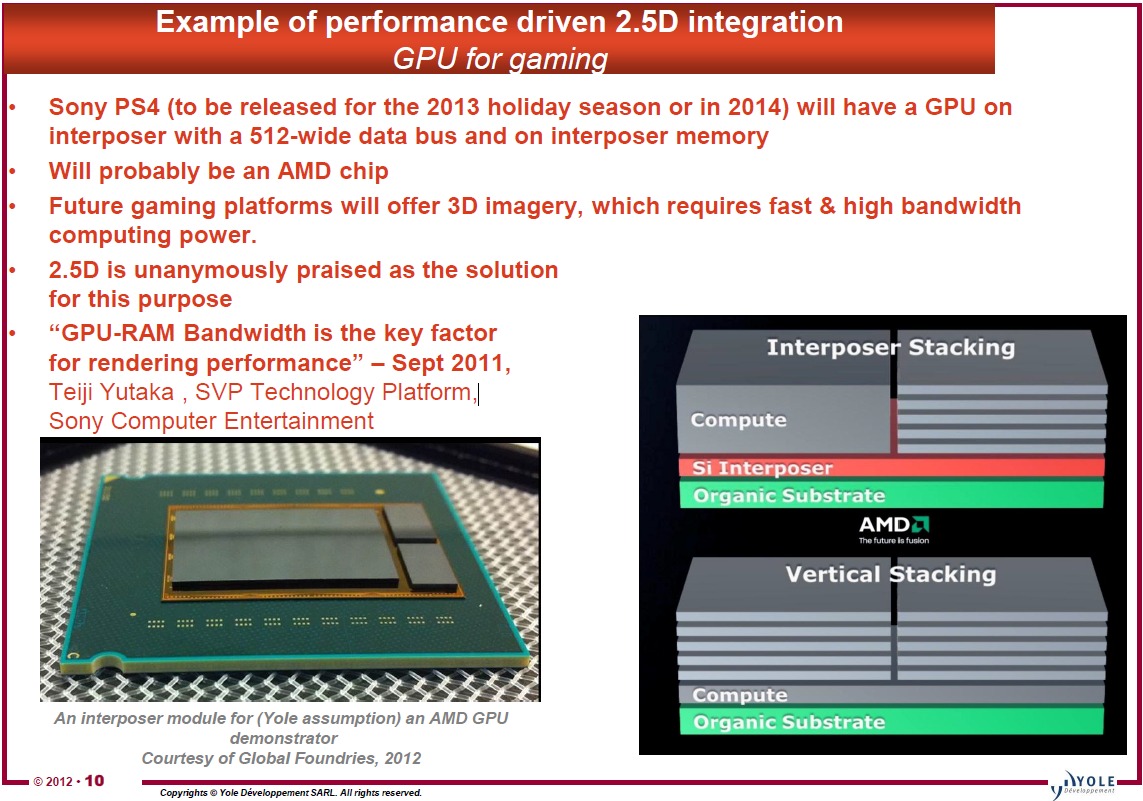
One of the advantages of using an interposer is that you can get very big bus width in an easier way ( shorter length of bus and less conections ). So if they use an interposer is more feasible it to have ddr3 stacked ( much less hot memory and less power hungry ) and conect it via interposer to a 512-1024 bits width interface to the APU and so reach the rumored near 193 GBs of bandwidth speed. See this:

http://semiaccurate.com/2011/10/27/amd-far-future-prototype-gpu-pictured/#.UPlJzh1hvZc

the PS4 kits could have GDRR5 at 193GBs only to approach the final silicom that could be made via stacked DDR3 memory and interposer ( IMHO something like this is what we will find in the launching console ).
 

Avtomat

Member
One of the advantages of using an interposer is that you can get very big bus width in an easier way. So if they use an interposer is more feasible it to have ddr3 stacked and conected via interposer to a 512-1024 bits width interface and so reach the rumored near 193 GBs of bandwidth speed.

My skepticism regarding the stacked memory on interposer is because no one else has done it in a high volume part to my knowledge. Intel the leader in process technology has not even debuted their implementation. However the rumour was Intel could have brought it to market last year with Ivybridge but decided against it for business and cost reasons, so it is not beyond the realm of possibility we could see it.

Having said that I believe you cannot get a huge amount of stacked memory (4GB) on an interposer but you will be able to get a reasonably small amount 32MB - 128MB which I can see happening. If this is the case replace my EDRAM speculation with that. Not really against it but I think both consoles will have localised high babdwidth smallish memory pools and a smaller amount of bandwidth out to main memory.
 

gofreak

GAF's Bob Woodward
Are you so sure there will not be...

Well nothing is for sure yet. But the noises are that these things are using APUs.

But my point is to think APU = A10-5800K is off base.

2 seperate dies sitting on a single interposer, as a 7870 is 212mm^2 adding another ~ 120mm^2 for a 4 core CPU @ 28nm

I assume the 120mm^2 estimate comes from the die area of the CPU in Trinity? That's on 32nm though and id Piledriver...and has twice the cache that was earlier rumoured for Orbis's 4-core/2-module CPU.

I'm not sure what the latest on Orbis's CPU is, but I don't think it'll be as big as that in Trinity.
 
Seems like the power difference is going to be marginal between the two. Third party games will roughly look the same and the true differences in performance will come down to first and second party companies. In that case, my money is on Sony.
 
My skepticism regarding the stacked memory on interposer is because no one else has done it in a high volume part to my knowledge. Intel the leader in process technology has not even debuted their implementation. However the rumour was Intel could have brought it to market last year with Ivybridge but decided against it for business and cost reasons, so it is not beyond the realm of possibility we could see it.

Having said that I believe you cannot get a huge amount of stacked memory (4GB) on an interposer but you will be able to get a reasonably small amount 32MB - 128MB which I can see happening. If this is the case replace my EDRAM speculation with that. Not really against it but I think both consoles will have localised high babdwidth smallish memory pools and a smaller amount of bandwidth out to main memory.

You can get a lof ot stacked RAM in a interposer. You maybe are talking about EDRAM?.
 

spisho

Neo Member
Sony just spent hundreds of millions of dollars releasing a handheld in a post iphone reality. They released move. They continue to put out first party titles that don't sell particularly well. They hitched their wagon to blu-ray and it cost them dearly.

Do I think Sony is incapable of making good decisions? No. Do I think there is a frequent crisis of vision there? Yes.

The post iPhone reality? Microsoft's ascendance? I think you're getting carried away with your prose a little.

It's easy to analyze a series of decisions in hindsight and pretend as if they were staggeringly obvious mistakes from the outset. The Vita, for example, takes a lot of flack for being a handheld console, and those things don't sell any more do they? (Hint: They do; Additional hint: everyone is making one these days.) Sony sold 70 million PSPs, and in Japan there's been a consistent trend towards portable gaming vs. home consoles. The Vita was previewed in Japan and launched first there, no mere coincidence. I'm also not convinced that handset gaming will eventually claim that market. Instead it exists as a separate but lucrative segment and Sony are making moves on the Android side with PSM.

I actually don't believe Sony are going with a small and fast pool of RAM. It doesn't fit the Vita model, and I'm sure they can come up with a memory hierarchy that provides fast bandwidth and additional slower RAM in higher capacities. Also, in no way do I think Sony are less competent than Microsoft at building a console. It's an engineering company with some of the most talented game developers in the world working for it. The only thing the PS3 demonstrates is that AMD would have been a better partner back in 2004, and well, lesson learned.
 
One of the advantages of using an interposer is that you can get very big bus width in an easier way ( shorter length of bus and less conections ). So if they use an interposer is more feasible it to have ddr3 stacked ( much less hot memory and less power hungry ) and conect it via interposer to a 512-1024 bits width interface to the APU and so reach the rumored near 193 GBs of bandwidth speed. See this:

http://semiaccurate.com/2011/10/27/amd-far-future-prototype-gpu-pictured/#.UPlJzh1hvZc

the PS4 kits could have GDRR5 at 193GBs only to approach the final silicom that could be made via stacked DDR3 memory and interposer ( IMHO something like this is what we will find in the launching console ).
That's the fall back using GDDR5 till the next refresh and that is possible except every professional cite says 3D stacked memory on Interposer will be used.

3) 3D wafer stacked memory will be ready for Game Consoles 2013-2014 Provides even more efficiencies when inside the SOC.

OBAN Japanese Coin

hist_coin13.jpg


The idea of the OBAN, a large blank substrate, to produce a large SOC. It can be custom configured and could be used in the PS4 and Xbox 720. This plus standardized building blocks produced by the consortium make sense. It makes sense of the various rumors. Arguments that this would be ready for this Cycle 2013-2014 have supporting cites.

http://semiaccurate.com/forums/showpost.php?p=164227&postcount=225 said:
That's why I keep posting 2.5D stacking news released by the company that Charlie's "Far Future AMD GPU Prototype" picture originated from. Moreover, Charlie made it rather clear that SONY is going for a "multi-chip-on-interposer" HSA design that is supposed to be gradually integrated into a cheaper, monolithic SoC later in the life cycle. We also heard about "two GPUs", so its probably going to be APU + dedicated GPU - with the APU-GPU basically reserved for GPGPU computation.

"Interposer inclusion defines the 2.5D approach. It will route thousands of interconnections between the devices. Coupled with true 3D stacked die (enabled by TSVs), the high routing density and short chip-to-chip interconnect ensures the highest possible performance while packing as much functionality as possible into the smallest footprint.

Functional blocks may include a microprocessor or special purpose logic IC (GPU, applications processor, ASIC, FPGA, etc.) connected through high-speed circuitry to other logic devices or memory (DRAM, SRAM, Flash) ..."

Memory of 2.5D and wide connections described are used in semiconductor research firm GPU [rumor], next generation of PS3 (PS4). This Sony lecture used as the basis of the ultra wide memory speculation.

http://www.i-micronews.com/upload/Rapports/3D_Silicon_&Glass_Interposers_sample_2012.pdf

95dd2b6d.jpg


Wild speculation but the Oban chip being made by IBM and GloFlo could be the BLANK (not populated) Transposer substrate for next generation. Oban is a blank oblong Japanese gold coin with bumps on it. Oban is also a Coastal town in northern England so who knows.

Good article linked in the above: Flow to the wide DRAM technology solutions to increase the momentum in the 2.5D

In summary, AMD not using 3D stacking at this point, will use 2.5D with interposer and implement wide I/O memory to get the memory transfer speed needed for Fusion chips. GDDR5 being replaced by ultra-wide RAM most likely DDR4.

HPC memory and graphics memory GDDR5 post for (High Performance Computing) is heading to the introduction of the technology of wide memory interface. It uses a technology solution: (Through Silicon Via TSV) through-silicon vias. However, it is said instead of DRAM stack directly on top of the CPU and the GPU, and are considering the introduction of a method to use the I / O chip and silicon interposer.

One of the plans that has emerged is a way to connect with a wide DRAM interface CPU and GPU silicon interposer technology using TSV. Called for the 3D stacking DRAM stacked directly on CPU and GPU, and how to use the interposer is 2.5D. As in the case of 3D stacking, ultra-wide interface can be used by a very large number of micro-bump pins. However, unlike 3D stacking, there is no need to use a TSV the GPU or CPU, in terms of reduced risk of manufacture.

By using ultra-wide interface, low power consumption, using the TSV solution can achieve ultra-wideband memory. Standards relatively quiet, "Wide I / O" is a wide interface for mobile DRAM, the bandwidth is 12.8GB/sec memory per chip. However, in ultra-wideband 4-8 times of Wide I / O, in a non-mobile, memory bandwidth is that you want to target are considering to 100GB/sec per chip. Development of Wide I / O These are sometimes referred to by the name Wide I / O and Ultra Wideband Wide I / O, such as computing Wide I / O.

From gofreak:

http://www.i-micronews.com/upload/3DPackaging/AC_3D Packaging_August2012_Web.pdf

Quote:
Sony’s next game station logic- on-interposer will reportedly similarly be fabbed by Global Foundries, and packaged by a collaborating OSAT ( Amkor).
Earlier in the year a panel of manufactuers (including Global Foundries), talking about 2.5/3D infrastructure, were asked if any of them would be supplying Sony for PS4.

http://www.electroiq.com/blogs/insi...ure-at-imaps-device-packaging-conference.html
 
The post iPhone reality? Microsoft's ascendance? I think you're getting carried away with your prose a little.

It's easy to analyze a series of decisions in hindsight and pretend as if they were staggeringly obvious mistakes from the outset. The Vita, for example, takes a lot of flack for being a handheld console, and those things don't sell any more do they? (Hint: They do; Additional hint: everyone is making one these days.) Sony sold 70 million PSPs, and in Japan there's been a consistent trend towards portable gaming vs. home consoles. The Vita was previewed in Japan and launched first there, no mere coincidence. I'm also not convinced that handset gaming will eventually claim that market. Instead it exists as a separate but lucrative segment and Sony are making moves on the Android side with PSM.

I actually don't believe Sony are going with a small and fast pool of RAM. It doesn't fit the Vita model, and I'm sure they can come up with a memory hierarchy that provides fast bandwidth and additional slower RAM in higher capacities. Also, in no way do I think Sony are less competent than Microsoft at building a console. It's an engineering company with some of the most talented game developers in the world working for it. The only thing the PS3 demonstrates is that AMD would have been a better partner back in 2004, and well, lesson learned.

Not to mention that a lot of his prose is flat out wrong. Sony's first party games have sold fine. People continue to trumpet that their exclusives are disappointments in terms of sales, but the Uncharted series was one of the biggest success stories this generation, God of War continues to be a monster, and Gran Turismo 5 is one of the biggest franchises in all of gaming (especially counting DLC or Prologue). Hell, even Heavy Rain did well. The Vita rumblings are bullshit. GAF has a history of dismissing Sony's products when in reality it just takes a while for them to get started. I recall many people saying that the PS3 was dead in the water and it would be less successful than the Gamecube. I think the Vita will be absolutely fine with a memory card packed in and a price drop.
 
the a10 thing is stupid. if sony shipped with an actual a10 theyd be fucked. alternatively, a a10 plus discrete gpu makes little sense despite what some want to believe (you'd be much better off making a discrete gpu bigger than having a second somewhat redundant one glued to the cpu)

pretty sure its just one of the just plain wrong rumors out there.
Why wouldn't it make sense again?
 
One of the advantages of using an interposer is that you can get very big bus width in an easier way ( shorter length of bus and less conections ). So if they use an interposer is more feasible it to have ddr3 stacked ( much less hot memory and less power hungry ) and conect it via interposer to a 512-1024 bits width interface to the APU and so reach the rumored near 193 GBs of bandwidth speed. See this:

http://semiaccurate.com/2011/10/27/amd-far-future-prototype-gpu-pictured/#.UPlJzh1hvZc

the PS4 kits could have GDRR5 at 193GBs only to approach the final silicom that could be made via stacked DDR3 memory and interposer ( IMHO something like this is what we will find in the launching console ).

Why the struggle for 4GB then? Shouldn't it be rather easy to stack 4 or 8GB of DDR3 memory? If you already use an interposer and stacking I guess it doesn't add much complexity or cost if you do it with 8GB instead of 2.
 
Why wouldn't it make sense again?

Because an APU plus GPU would be messy, both from a manufacturing standpoint (two kinds of RAM, more complicated motherboard), and from a development standpoint (multiple RAM pools to manage, multiple GPUs to target, no efficient way to get them to work together).

Why the struggle for 4GB then? Shouldn't it be rather easy to stack 4 or 8GB of DDR3 memory? If you already use an interposer and stacking I guess it doesn't add much complexity or cost if you do it with 8GB instead of 2.

If they indeed get stacked memory on an interposer ready, 8GB is totally in reach, which is why it's premature to be passing judgement on Orbis and Durango at this point. 4GB is only the hard limit if they're stuck using GDDR5 on a 256 bit bus. 4GB may just be the limit of what they can do in the development hardware, using GDDR5 to simulate the bandwidth of the Wide I/O stacked memory.
 

Nachtmaer

Member
The way I see it, Sony might be going for one of these set ups:


  • A Richland APU + dedicated GPU. Richland is basically a refreshed Trinity and a stopgap for Kaveri allowing higher clock speeds and perhaps bringing other functionalities we don't know yet.

  • A Kaveri APU + dedicated GPU. If GloFo gets its process working well enough, perhaps AMD might give Sony priority over the PC market for these chips. Like the previous set up, they could use the APU's GPU for GPGU tasks. They could also use just the APU for movie playback and whatnot, saving power when the dedicated GPU isn't needed.

  • One big APU consisting of Piledriver, Steamroller or Jaguar cores with a somewhat beefy GPU with the needed HSA functionalities. Personally I hope they choose this option. It might not be the cheapest one R&D-wise but it could save a lot of trouble in the long run. Perhaps it even allows a cheaper box since you don't have to deal with two chips needing to be fed and you only need to shrink one chip in the future.

From what I've gathered, going with an interposer and 2.5D stacked DDR3/DDR4 won't be much of a cost saver vs GDDR5 for now, but it does give you more TDP headroom for other parts.
 
Why the struggle for 4GB then? Shouldn't it be rather easy to stack 4 or 8GB of DDR3 memory? If you already use an interposer and stacking I guess it doesn't add much complexity or cost if you do it with 8GB instead of 2.

They can give devs only the RAM amount which they can guarantee - if stacking will not be ready in time, they would have to launch with GDDR5, and they can't use more than 4 GB GDDR5.
 

TheOddOne

Member
CVG sources: Sony to abandon DualShock design for PS4
PlayStation will bring an end to a sixteen-year tradition of DualShock controllers with the release of the PlayStation 4, CVG has learned.

All PlayStation controllers have undergone extensive prototyping A senior games studio source working on an upcoming Sony game says the new system's controller has undergone numerous iterations, few of which resemble the DualShock build that has become synonymous with PlayStation.

Experiments within Sony's R&D department are thought to have been extensive. Versions of the new PS4 pad include biometric sensors on the grips and an LCD touch screen, the development source claimed.

A second source, working in a separate part of the industry but still connected to Sony, said PlayStation engineers are "trying to emulate the same user interface philosophies as the PS Vita". This is likely a reference to the touch-screen capabilities of the PlayStation handheld, and a suggestion that Sony will tightly integrate its portable and home systems.

The new console - codenamed Orbis - will be revealed in a matter of weeks, not months.

Sony has declined to comment.

While the DualShock will not be a primary controller for the next PlayStation, it is likely that the range of PS3 controllers will be compatible with the next-gen system. There is a possibility they could be used as secondary controllers, much like with how Wii Remotes interact with the Wii U.

One potential stumbling block is Sony's complex partnership with Immersion - the patent-holder of the rumble tech used in Sony's pads. In March 2007, Immersion settled its patent infringement suit with Sony, after claiming that the company had used its technologies without permission.

CVG understands that Sony has paid Immersion more than $150 million in damages, license fees and other costs since the settlement. However, a small portion (initially $20 million) of this was redirected to Microsoft, which owns about 10 per cent of Immersion.

Sony's licence agreement with Immersion ends in 2017, SEC documents show, but as part of the deal Immersion has given Sony an option to expand the scope of the licence for future consoles. However, the complications of the deal may have convinced Sony that it should seek different designs and ideas for its next controller.

Sony introduced the DualShock for the first PlayStation in 1997 - its twin analogue sticks were, at the time, considered a distinct improvement over the N64 pads from rival Nintendo.

Over the years, the controller has evolved to include rumble tech (as well as briefly omit it), as well as add on wireless capabilities and limited motion control properties.

In 2007 Sony won an Emmy award for 'Peripheral Development and Technological Impact of Videogame Controllers'.

The new PS4 controller design, which remains a closely guarded secret across the PlayStation organisation, is expected to break new mould for Sony. The biometric tech, in particular, is something games studios such as Valve are interested in due to its function as a heart beat sensor.

During the development of the PlayStation 3, Sony initially signalled its interest in building a new controller by showcasing the infamous 'banana pad' - a model that was swiftly replaced by the DualShock following public derision.
 
Because an APU plus GPU would be messy, both from a manufacturing standpoint (two kinds of RAM, more complicated motherboard), and from a development standpoint (multiple RAM pools to manage, multiple GPUs to target, no efficient way to get them to work together).


.

There's nothing that says there would have to have to be two pools of ram, you are assuming. And pretty much everything you say about the development standpoint is baseless speculation.
 
From what I've gathered, going with an interposer and 2.5D stacked DDR3/DDR4 won't be much of a cost saver vs GDDR5 for now, but it does give you more TDP headroom for other parts.

Often you have to take a long view with hardware designed to be in active production for 10+ years. GDDR5 could be cheaper now than a DDR3/4 stack on interposer, but a couple years from now the GDDR5 will probably be a lot more expensive, and 7 years from now the GDDR5 could be prohibitively expensive (since the industry has long moved on to newer, better memory tech and no one wants to make it anymore).
 
I guess they could integrate a touchpad on the back for using the web browser or something like that. Whatever it is, I hope it isn't too expensive. And an announcement in the next time would be incredible.
 

Ashes

Banned
Because an APU plus GPU would be messy, both from a manufacturing standpoint (two kinds of RAM, more complicated motherboard), and from a development standpoint (multiple RAM pools to manage, multiple GPUs to target, no efficient way to get them to work together).

Two kinds of ram?
 
Secret sauce everyone has been missing http://blogs.amd.com/fusion/2012/03...ia-experience-for-our-“connected”-generation/

Why are we thinking that post processing AA will be needed? No one has looked at this and speculated that hardware based AA is already built into the AMD hardware:

Here’s what you can expect from your next PC multimedia experience, thanks to the AMD HD Media Accelerator found in “Trinity” APUs:

Rich, clear HD video: AMD Perfect Picture HD, an image, video processing and display technology that automatically makes images and video better with color vibrancy adjustments, edge enhancement, noise reduction and dynamic contrast fixes.[iii]

Virtually uninterrupted video streaming: Tired of waiting for streaming videos to “buffer”? If so, you will appreciate AMD Quick Stream technology. Now, you can enjoy smoother, virtually uninterrupted video streaming to watch what you want, when you want.[iv]

Virtual push-button shaky video stabilization: AMD Steady Video technology is an exclusive feature based on AMD Accelerated Parallel Processing Technology designed to eliminate shakes and jitters during the playback of home video. Following a successful introduction last June, the next generation of AMD Steady Video technology will now be delivered via a light-weight web browser plug-in to watch streamed video on the most popular browsers, as well as for your videos stored locally.[v]
Upper right in this picture of an OLDER Trinity. AMD HD Media Accelerator. It's post processing a video image and cleaning it up, it can detect edge and noise.

HSAAcceleratedProcessingUnit.png
 

Avtomat

Member
You can get a lof ot stacked RAM in a interposer. You maybe are talking about EDRAM?.

I have seen little indication of exactly how much stacked RAM you can get away with but the little speculation I have seen for Intel strongly suggested 64MB from Anandtech and up to 128MB from Charlie at Semiaccurate. I believe Anand is closer to Intel on these things. Secondly putting such a large amount of RAM so close to your processing centres may mean a worsening of thermal conditions.

Well nothing is for sure yet. But the noises are that these things are using APUs.

But my point is to think APU = A10-5800K is off base.


I assume the 120mm^2 estimate comes from the die area of the CPU in Trinity? That's on 32nm though and id Piledriver...and has twice the cache that was earlier rumoured for Orbis's 4-core/2-module CPU.

I'm not sure what the latest on Orbis's CPU is, but I don't think it'll be as big as that in Trinity.

Yup that is an estimate based on Trinity, trying to factor in the shift to 28nm and a reduction in L2 cache (assuming 1MB per module) I guess you would come in at around 90 - 100mm^2 remember steamroller cores are actually slightly more complex due to the rework of the decoder at least.

If they are targetting something around the size of pitcairn for the GPU side of things you would still be looking at ~300mm^2 yes they could get by with disabling CU's and the like but my gut tells me it would be better to go with 2 seperate dies with an aggresive move down to 20nm before looking at integration on a single die.

Definitely agree has to be better than a 5800k.
 
aegies said:
I was most concerned about memory bandwidth on the system, because I was worried they were going with something slow.

I'm no longer concerned about that.
aegies said:
And maybe developers on Microsoft's end were given a hypothetical situation where they could speak out in favor of DDR5 or twice as much relatively fast DDR3 + ED-RAM plus ... some other stuff that, you know, MAYBE mitigates the bandwidth "deficiency" that could present itself in that situation

Looking forward to finding out the details of the various elements of the Nextbox hardware and getting a better idea of what's going on there. It certainly feels like we're missing the full picture in these RAM debates.
 
There's nothing that says there would have to have to be two pools of ram, you are assuming. And pretty much everything you say about the development standpoint is baseless speculation.

Except that off the shelf APUs and GPUs have their own memory controllers and aren't set up to interface for UMA. And we know what integrated + discrete GPU crossfire looks like and it's really inefficient. If the theory is Sony just wants to combine off the shelf parts with minimal changes, it will be less elegant, and less efficient than a high performance single APU with the kind of HSA advantages that brings.
 

Nachtmaer

Member
Often you have to take a long view with hardware designed to be in active production for 10+ years. GDDR5 could be cheaper now than a DDR3/4 stack on interposer, but a couple years from now the GDDR5 will probably be a lot more expensive, and 7 years from now the GDDR5 could be prohibitively expensive (since the industry has long moved on to newer, better memory tech and no one wants to make it anymore).

Yeah exactly, that's why I said for now. I guess the PS3's XDR is a good example of that as well.

And we know what integrated + discrete GPU crossfire looks like and it's really inefficient.

Even AMD promotes crossfiring an APU with only a low end discrete GPU. Using it with a let's say a 7800-class GPU probably causes more harm than good.
 
Secret sauce everyone has been missing http://blogs.amd.com/fusion/2012/03...ia-experience-for-our-“connected”-generation/

Why are we thinking that post processing AA will be needed? No one has looked at this and speculated that hardware based AA is already built into the AMD hardware:


Upper right in this picture of an OLDER Trinity. AMD HD Media Accelerator. It's post processing a video image and cleaning it up, it can detect edge and noise.

HSAAcceleratedProcessingUnit.png

That sounds like one of those rather useless "features" most TVs have which I disable during gaming. For home cinema experience I rather have a THX certified picture instead of something every PC can do and AMD desperately tries to sell as innovation.

Every Intel Core iX CPU + Media Player Classic can do the same or is superior...
 
Except that off the shelf APUs and GPUs have their own memory controllers and aren't set up to interface for UMA. And we know what integrated + discrete GPU crossfire looks like and it's really inefficient. If the theory is Sony just wants to combine off the shelf parts with minimal changes, it will be less elegant, and less efficient than a high performance single APU with the kind of HSA advantages that brings.

Who says anything about off the shelf APUs? When does that become law regarding custom hardware? Sony is a very capable hardware manufacturer, they are far from being someone who has no choice but to accept whatever AMD decides to give them. "SLI" or "crossfire" has no bearing here.

They have patents for this type of thing and in the drawing there is only one memory controller, albeit two pools of ram. The data flow looks pretty solid too. You're gonna have to come with alot better reasoning besides "but look at how pcs do it" to convince me. Especially if you are lacking any EE experience.
 
That sounds like one of those rather useless "features" most TVs have which I disable during gaming. For home cinema experience I rather have a THX certified picture instead of something every PC can do and AMD desperately tries to sell as innovation.

Every Intel Core iX CPU + Media Player Classic can do the same or is superior...
Yup and likely why it's been dismissed or not thought of but AA is a hog and the above uses several algorithms that AA uses and it's hardware based. If it can detect an edge and noise it can be tuned to do AA. The worth less feature you turn off caused me to wonder at all the AA issues others were commenting about as I didn't have them on my 2008 Samsung DLP and it was the very top end with TI video processing. When I connected my PS3 to a cheaper TV I seriously noticed the AA issues in older games.

If you can force developers to support 1080P you can probably get very good performance out of the built in HD Media accelerator to eliminate aliasing.
 
Secret sauce everyone has been missing http://blogs.amd.com/fusion/2012/03...ia-experience-for-our-“connected”-generation/

Why are we thinking that post processing AA will be needed? No one has looked at this and speculated that hardware based AA is already built into the AMD hardware:


Upper right in this picture of an OLDER Trinity. AMD HD Media Accelerator. It's post processing a video image and cleaning it up, it can detect edge and noise.

HSAAcceleratedProcessingUnit.png

Dude that's for video, AMD Perfect Picture HD is AMD's equivalent to Nvidia's Pure View really has nothing to do with videogames. AMD already has a post process based AA that detects edge and noise, MLAA. It's been a part of AMD's cards since Catalyst 12.4.
 
Top Bottom